
Simulate Flex Circuit PCB Performance
Unlike conventional PCBs, flex circuits are capable of bending and re-bending. This re-bending, coupled with the stress of moving components, can lead to board failure. It is important to understand the physics of this behavior and plan for it in advance. To do this, a designer should use simulation software to determine how a flex circuit will perform under different conditions. This way, potential problems can be addressed before moving on to material fabrication.
The most obvious consideration is the allowable bending radius for the flex section. The bending radius can be calculated using the allowed deformation of copper on the outer edge of conductors. This can be influenced by the layer count, type of copper (RA or ED), and other materials. A flex circuit with a hatched copper plane is more flexible than one with solid copper pours. In addition, a hatched pattern can help to distribute copper stresses more evenly. The best choice is a hexagonal hatched pattern that minimizes the bias in 0deg, 90deg, and 45deg angle directions.
A flex circuit design should also consider the number of layers and whether it will include a rigid section. If the flex circuit is static, it can be designed with more layers and thicker copper. However, it is important to remember that the stiffener will also influence bending flexibility.
Another consideration is whether to use an adhesive-based or adhesiveless substrate. The latter has the advantage of being easier to assemble. It is also more environmentally friendly, but it requires a longer cure time. Regardless of the choice, a designer should consult their fabricator with a proposed stackup to ensure that it can be reliably fabricated.
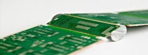
How to Simulate Flex Circuit PCB Performance
Drill-to-copper distance is another important factor to keep in mind. Since flex materials are more likely to move and compress during production, it is best to leave a gap of at least 8 mil between the drill and the copper. In addition, a flex circuit should have end cutouts or slits in accordance with IPC to reduce tearing of the corners.
Lastly, a flex circuit should be designed to avoid copper overlaps. The stress of overlapping traces can cause the flex circuit to break. To prevent this, a flex circuit pcb should be designed with staggered traces.
Additionally, designers should be aware of the difference between panel plating and pad-only plating (button plating). The former has a greater versatility in that it allows manufacturers to control copper thickness and improve etch yields in intricate etch patterns. It is more expensive, however, because of extra processing steps.
Therefore, it is best to choose button plating when possible. However, if a designer needs to utilize panel plating for a specific application, the board should be built with anchors at the ends of the pads. This will prevent them from becoming detached during re-bending. The anchors can be added in the top solder mask layer, or they can be defined in a separate coverlay opening. In either case, the anchors must be anchored in the copper, as opposed to being deposited on the pad itself.