
PCB HDI for High-Frequency
PCB HDI is a technology that allows for higher-density circuit boards with improved performance. It is used in applications such as automotive electronics, computer peripherals, and high-speed communication devices. While HDI is a key component of modern technological advancements, it poses many challenges when designing for high-frequency applications. This article explores the impact of HDI on signal integrity and transmission quality, as well as groundbreaking manufacturing techniques tailored to these types of applications.
High-speed HDI designs require special considerations to avoid a host of PCB layout pitfalls, including signal interference and crosstalk, ground bounce, signal ringing, and impedance mismatches. These problems can be addressed by utilizing strict design guidelines and following accurate circuit board design processes. This includes using the shortest possible trace widths, creating consistent impedance paths, and providing sufficient ground planes.
The use of pcb hdi technology in high-speed applications also requires careful attention to power distribution. The power rails must be properly sized to handle the increased current, while taking into account parasitic inductance and capacitance. This can be done by utilizing proper power management techniques and performing EMI modeling during the design phase.
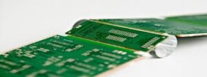
PCB HDI for High-Frequency Applications
Another major challenge for HDI technology is the need to use high-quality copper plating methods. This ensures the reliability of plated microvias, which serve as connections between different layers. In addition, the dielectric material must be capable of surviving thermal shocks during assembly, as well as maintaining its integrity after multiple reflow and soldering cycles.
Lastly, HDI circuit boards must be designed with the right fanout strategy. This will help reduce the number of sequential laminations, which in turn will reduce the cost and weight of the finished product. In addition, the HDI stack-up should be chosen with the proper density and layer spacing. This will prevent excessive signal interference due to unused pins or pads.
The metallization process plays an essential role in the production of HDI circuit boards, and is crucial to their performance. This is because it determines the quality of the plated copper, which directly affects signal propagation. Ideally, the thickness of the deposited copper should be above 0.6 microns. This will provide good conductivity and durability, as well as prevent the oxidation of the conductive surface.
In addition to the proper metallization process, the dielectric material used in HDI circuit boards must be capable of supporting the formation of plated microvias. The plated microvias must be robust and reliable, which can be achieved through the utilization of either electroless or electrolytic copper plating.
Additionally, the copper must be of high-quality in order to resist corrosion and other environmental factors. This can be accomplished by incorporating a pre-cleaning method into the fabrication process. The pre-cleaning method removes impurities and contaminants from the surface of the conductive metal, which can lead to a more durable and reliable product. The pre-cleaning method can be performed by using plasma treatment or chemical etching. The result is a more durable and reliable product that can withstand harsh environments, such as those found in aerospace and military applications.