
design challenges in flexible PCB fabrication
PCBs are the foundation of any electronics assembly. They provide the electrical path between components and enable devices to withstand environmental stresses like mechanical shock and thermal variation. With the rise of new technologies such as foldable smartphones and wearable electronics, engineers face a unique challenge of balancing functionality with durability. PCBs must be lightweight, thin and flexible to adapt to changing environments and user needs. This is where flexible circuit boards (FPCs) offer significant advantages – they significantly reduce the size and weight of devices, while enhancing their reliability.
Flexibility can also improve functionality, enabling devices to bend and conform to different shapes and sizes. However, the flexibility of FPCs introduces a set of additional design challenges that must be addressed to maintain their reliability and performance. These include ensuring the proper transition of signal layers between rigid and flexible sections, maintaining signal integrity, and keeping impedance levels within the required tolerances.
One of the most common types of issues that flexible pcb fabrication experience are problems with solder mask/coverlay openings and the alignment between the copper plating layer and the rigid board. These issues occur as a result of the complex processes that go into creating a custom flex PCB, including copper plating, etching and pumice scrubbing. These effects can make it difficult for the solder mask/coverlay to stay in place, which can lead to the formation of stress points and cracks in the solder joints.
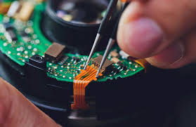
What are the design challenges in flexible PCB fabrication?
Another important issue is the use of different materials for rigid and flexible parts, which can create issues with thermal expansion/contraction that can impact flex PCB stability. The proper material selection can avoid these issues by providing better bending and reliability characteristics.
A final common problem is improper connector placement on a flex PCB, which can lead to mechanical failure. This type of issue is often caused by the lack of a sufficient minimum bend radius in dynamic flex areas. For a flex PCB to perform properly in its intended application, the maximum dynamic flex radius should be at least 100X the finished thickness of the board in these areas.
The impact of flexible PCB fabrication on circuit performance is highly application-dependent. In high-frequency applications, such as RF circuits and antennas, the lower dielectric constant of flexible substrates is advantageous for minimizing signal loss. In medical devices and wearables, the mechanical reliability and lightweight nature of flexible PCBs are critical for patient comfort and device performance. In automotive and aerospace applications, flexible PCBs offer space-saving benefits and are suitable for environments with significant vibration or temperature fluctuations.
Fortunately, innovations such as laser direct imaging, roll-to-roll lamination and conductive inks have helped refine flexible PCB fabrication. These advances have enhanced trace patterning accuracy, allowing for the creation of dense circuits in dynamic flex areas. They have also improved the speed of fab processing, and lowered production costs. In addition, conformal coatings can protect assemblies from moisture and other contaminants. Using these techniques, XPCB LIMITED can deliver high-quality flex PCBs that meet or exceed the requirements of most applications. To learn more about our flexible PCB manufacturing services, please contact us. We look forward to partnering with you!