
key design considerations for an RF circuit board
Designing a Radio Frequency (RF) circuit board involves a complex set of considerations to ensure optimal performance, signal integrity, and reliability. RF circuit boards are integral to applications in wireless communication, radar systems, satellite technology, and consumer electronics, all of which require precise signal transmission over high frequencies. A slight error in design can result in significant performance degradation, signal loss, or interference. Therefore, it is essential to take into account several key factors during the design process to create a high-performing and robust RF circuit board.
One of the most critical design considerations for an RF circuit board is signal integrity. As RF signals operate at high frequencies, they are highly susceptible to noise, interference, and distortion. Ensuring signal integrity requires careful attention to the layout of the circuit board to minimize unwanted effects such as signal reflection, crosstalk, and electromagnetic interference (EMI). The traces on the board should be designed with precise impedance control to maintain a consistent signal path. Inconsistent impedance can lead to reflections, where part of the signal is sent back toward the source, resulting in data loss or degradation. To manage this, controlled impedance traces and proper grounding are essential to maintain the high fidelity of RF signals.
Another important factor in rf circuit board design is material selection. The materials used for the substrate and the conductive traces greatly influence the electrical performance of the board, particularly at high frequencies. The most commonly used substrates in RF boards are PTFE (polytetrafluoroethylene), ceramics, and FR4. PTFE and ceramics are preferred in high-performance applications due to their low dielectric constants, which result in reduced signal loss. The dielectric material between the conductive traces determines the speed at which signals travel through the board and affects factors like signal delay and reflection. Choosing the right material ensures that the RF board performs well at the specific frequencies for which it is designed.
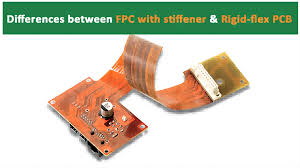
What are the key design considerations for an RF circuit board?
The size and layout of the circuit board also have a significant impact on performance. In RF designs, compactness and the strategic placement of components are essential to minimize path lengths and reduce signal attenuation. The placement of components such as resistors, capacitors, inductors, and active devices must be optimized to prevent signal degradation and interference. Additionally, careful routing of RF traces ensures that the signals do not travel through areas of the board that are prone to unwanted coupling or noise. It is important to maintain adequate spacing between components and traces to prevent interference and to allow for efficient heat dissipation.
Thermal management is another key design consideration for RF circuit boards. As RF systems operate at high frequencies, they generate significant amounts of heat, especially in high-power applications such as transmitters and power amplifiers. Excessive heat can degrade the performance of components and even cause failure. To address this, RF circuit boards should be designed with thermal management strategies in mind. This includes using materials with good thermal conductivity, incorporating thermal vias to direct heat away from sensitive components, and adding heat sinks where necessary. Effective thermal management ensures the longevity and reliability of the board, even under demanding operating conditions.
Grounding and shielding are also crucial in RF circuit board design. A proper grounding system reduces the impact of EMI and ensures the stability of the RF signals. Ground planes, typically made of copper, are used to provide a low-impedance path for returning current. These ground planes should be continuous and unbroken to avoid noise and interference. Additionally, shielding is used to prevent external electromagnetic fields from affecting the signals on the circuit board. Shielding can be achieved by enclosing sensitive components with metal casings or using special shielding materials.
Finally, design for manufacturability and testability is essential to ensure that the RF circuit board can be reliably produced and tested in a cost-effective manner. This includes considering factors such as component availability, ease of assembly, and the ability to perform in-circuit testing to verify signal quality. A well-designed RF circuit board should be easy to fabricate, with clear documentation and design rules that facilitate production.
In conclusion, designing an RF circuit board involves numerous considerations that impact its performance and reliability. Key factors such as signal integrity, material selection, layout, thermal management, grounding, and manufacturability must all be carefully addressed. By optimizing these design elements, engineers can create RF circuit boards that meet the stringent demands of high-frequency applications, ensuring robust and efficient operation in a variety of industries.